Building my own keyboard - Part 8
Redesigning the board
The choice to temporarily move to the Holtek controller means that I have to redesign the whole board so that the matrix complies with the controller expectations. I took also the chance to redesign the layout and baseplate to the expected new keycap sizes (space 2.75).
Then, I mapped each key to the appropriate row and column. First the left part
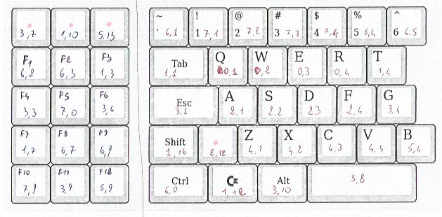
And then the right part
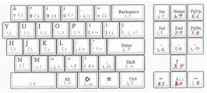
Now, the bad news is that the assignment is far from straightforward, and both left and right use a very large number of columns, meaning that the cables that will go from the matrix to the controller will have 28 contacts (8 rows and 20 columns), most of which will be used. If I had a better, more partitioned assignment I could have had cables with less contacts, but this is not the case, so I decided to make the contact uniform for both left and right. Pin 1-8 are R0-R7, and Pin 9-28 are C0-19.
The complicated assignment given above will also mean a very messy PCB routing, which is what I am going to do next: I fired up EasyEDA ready to endure the pain, but I realised an additional puzzling question.
In my previous PCB, I added diodes, which is a common way to prevent ghost keys. The Holtek controller datasheet makes no mention of it, which means that it has internal ways of dealing with the problem, but reusing my old matrix made me realise that I did not understand the internal design of the Holtek. It appeared that my diode would backwards, as the Column pin is an output and the Row pin is an input. My diode goes in reverse, I thought, because I expected the current to go from the output to the input.
I posted the question on Electronics SE, and I didn’t get an answer because that’s the way things are on SE sites, but one user wrote an insightful comment that it works in reverse: the C pin is high, and gets pulled low by the scan. The row input pins have an internal pull-up, meaning that they are always high unless pulled low by the column pin. Of course, this cannot happen if the column pin is not connected. When you press the button, and the column pin goes low, the row pin is pulled low as well, and this is allowed by the diode as I designed it in the old matrix.
I plugged the logic analyser to the Holtek and powered it up. This is the result:
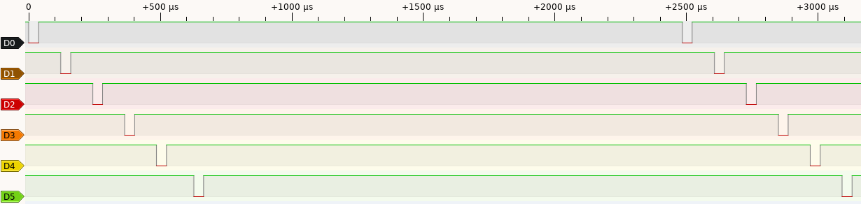
The image shows six column pins C0-C5. They are always high, and the controller pulls them low for around 40 microseconds, and switches to a new column after around 80 microseconds. The entire cycle through the 20 column pins is done in around 2500 microseconds. I don’t have more accurate timings as I am only checking the above picture and I didn’t bother to measure them accurately after the scan. It’s not that important, but it gives an idea of the speed of the scan.
As an additional check, I tried to desolder the diode and connect it backwards, and sure enough, the button stopped working.
So the take home messages are:
- there are things the datasheet doesn’t say
- SE sites are pretty much useless in finding people that want to help you. Instead, they criticise what you are doing, how you are doing it or how you present it. Only occasionally you find the rare comment that gives you an insightful hint, but you are mostly on your own. If you are a beginner or inexperienced, you won’t learn anything by asking on SE.
- I technically don’t need the diodes for the Holtek chip (probably it has them internally), but I will add them anyway because my controller will need them. The Holtek won’t care, as long as they are in the same configuration they are in now: Row -> button -> diode -> Column.
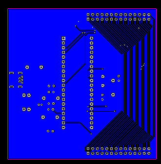
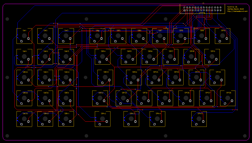
Nevertheless, I pushed forward with the routing, and I obtained three new PCBs. The left board
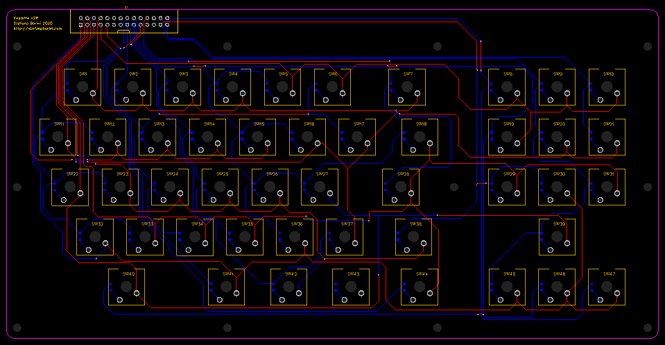
The right board
and the new controller board, which now accepts all lines (the first version accepted only a limited number of them), top:
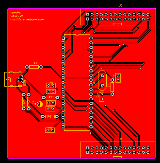
and bottom (note the huge number of lines to connect both left and right halves to the same pins)